Optoelectronics Group possesses the infrastructure for wafer processing, testing and sophisticated characterization of optoelectronics devices. Move mouse over the thumbnails below to get a larger view and complete information on each facility.
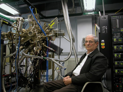
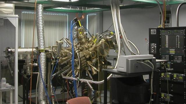
Veeco GEN 930 MBE system
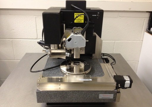
Veeco diDimension V AFM
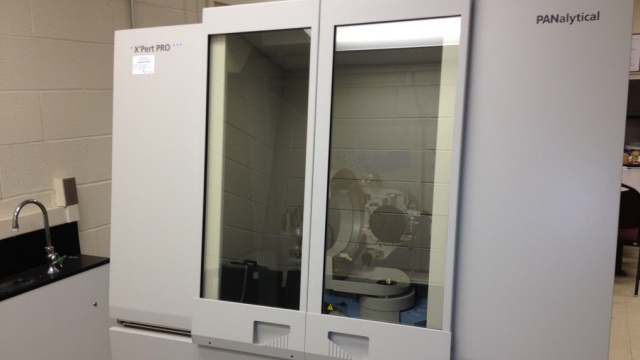
PANalytical X-ray diffraction system
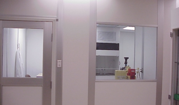
Class 100 clean room
Karl Suss MJB3 mask aligner
OAI dual side mask aligner
Trion PECVD
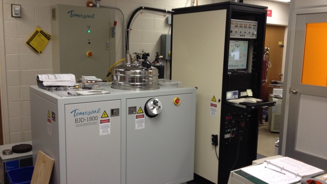
Temescal BJD-1800 E-beam deposition system
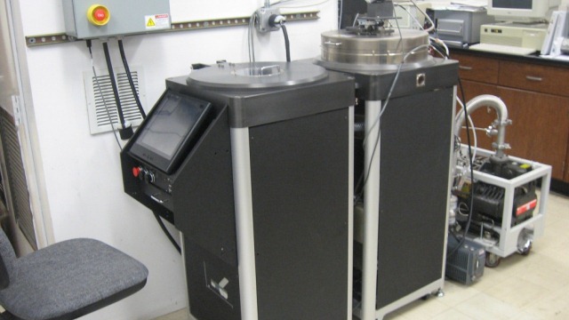
Trion ICP-RIE
WEST BOND wire bonder
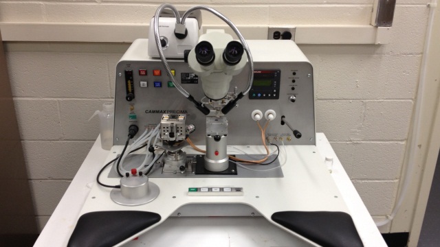
CAMMAX Die bonder
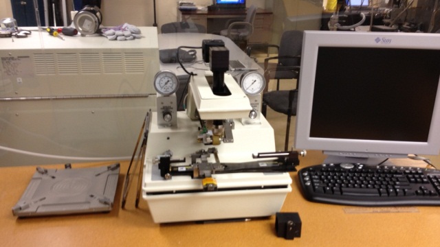
Loomis Die scriber
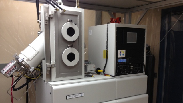
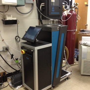
Denton Exploer E-beam thin film deposion system
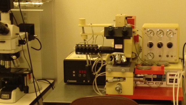
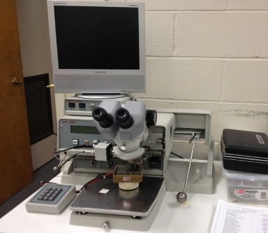
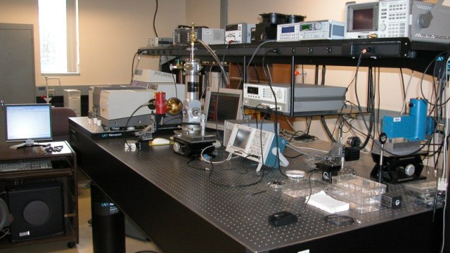
Device characterization bench
Device characterization bench
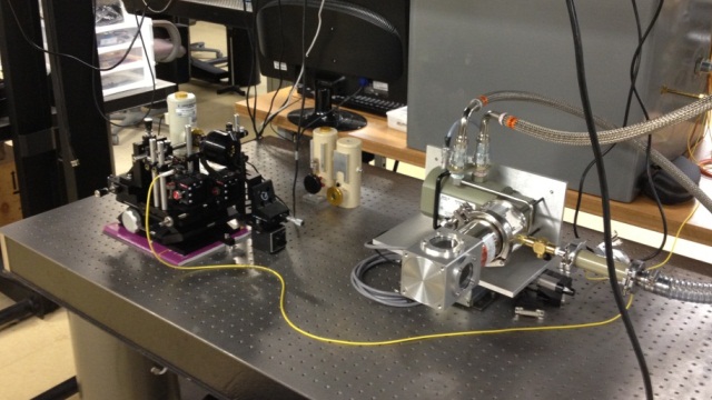
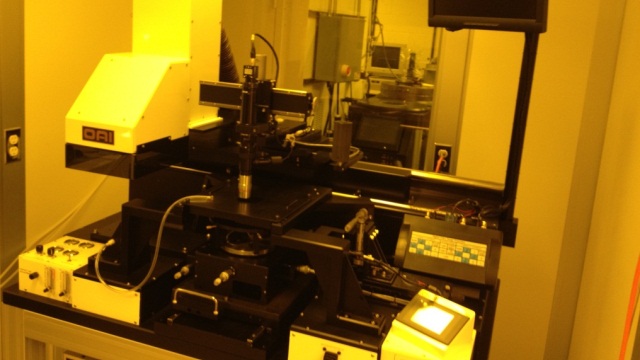
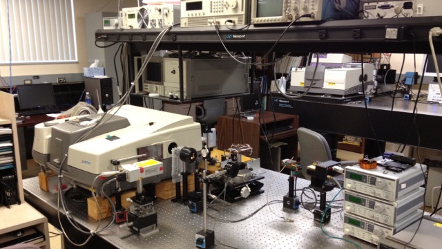
Frequency-modulated photoluminescence response measurement setup
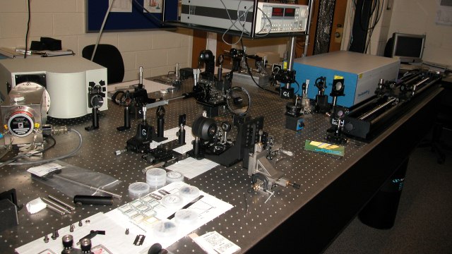
Ultrafast lab